GaAs Analysis#
Calculation Details#
- Comparison of electronic states in GaAs with As defects under neutral and electron-doped conditions.
Target Structure#
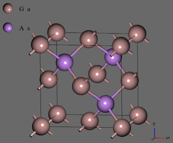 Zincblende structure incorporating As defects (a=5.65Å) |
Calculation Conditions#
The same values were used for all parameters common to AOF-DFT and KS-DFT.
| Parameter | Value |
|---|---|
| Pseudo-atomic orbital | Ga7.0_as.pao, s1p1 As7.0_as.pao, s1p1 |
| Pseudopotential | Ga_PBE26_as.vps, As_PBE26_as.vps |
| Functional model (AOF-DFT only) | Crystal26 |
| Energy cutoff | 150 Hartree |
| k-point density (KS-DFT only) | 3.5 point/Å-1 |
| Smearing width | 0.02 Hartree |
| Convergence threshold | 1.0×10⁻⁶ Hartree |
| total charge | 0.0 or -1.0 |
Calculation Results#
- Upon charge doping, the variation in Mulliken charge, Δq, is almost twice as large on Ga atoms compared to As atoms, which correctly represents the localization of the doped electrons onto the Ga atoms around the vacancy.
| AOF-DFT | KS-DFT | |
|---|---|---|
| Δq of Ga | -1.72e-01 | -1.82e-01 |
| Δq of As | -1.04e-01 | -9.07e-02 |
- The calculated electron density can be exported to a cube file, enabling visualization with external tools like NanoLabo.
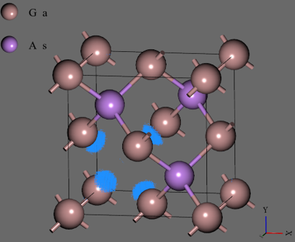 AOF-DFT visualization of electron density differences between doped and neutral states(only values of rhomax x 0.9 or greater) |