Interface Energy Calculation Using M3GNet#
In this case study, M3GNet was applied to interface model and surface model and compared to DFT calculations in terms of energy although it was optimized for bulk structures.
Energy Calculation for Bulk Model#
To calculate surface and interface energies, bulk model energies were calculated in the first place. The structures were imported from Materials Project(https://materialsproject.org/). The structures were optimized using M3GNet with anisotropically deforming the cell, then the energies were calculated using M3GNet and Quantum Espresso, respectively.
The number of k-points can be specified in Quantum Espresso's SCF calculation. This time, it was set so that (Cell Size)×(k-points)≈25.
| Al | Al2O3 | AlN | Au | GaN | Pt | Si | SiC | SiO2 | Ti | TiN | TiO2 | W | ZnO |
|---|---|---|---|---|---|---|---|---|---|---|---|---|---|
| mp-134 | mp-1143 | mp-661 | mp-81 | mp-804 | mp-126 | mp-149 | mp-8062 | mp-8059 | mp-72 | mp-492 | mp-390 | mp-91 | mp-2133 |
Surface Energy for Slab Model#
Analysis Procedure#
M3GNet was applied to surface models of several materials. The surface structures with vacuum layers on the top and bottom were optimized using M3GNet with the cell fixed, then the energies were calculated in M3GNet and Quantum Espresso, respectively. The surface energies were calculated by subtracting the bulk energies by the number of atoms from the energy of the slab structure.
Structure Creation#
Advance/NanoLabo feature made it easy to create slab models. Because the atoms displayed in the checkerboard pattern had fixed coordinates, they were unfixed by using Advance/NanoLabo feature.
The following table shows the surface orientation of the surface structures created.
| Material | Slab 1 | Slab 2 | Slab 3 |
|---|---|---|---|
| Al | (001) | (011) | (111) |
| Au | (001) | (011) | (111) |
| Pt | (001) | (011) | (111) |
| W | (001) | (011) | (111) |
| Si | (001) | (011) | (111) |
| SiC | (001) | (011) | (111) |
| SiO2 | (001) | (011) | (111) |
| TiN | (001) | (011) | (111) |
| TiO2 | (001) | (011) | (110) |
| Ti | (001) | (100) | (110) |
| AlN | (001) | (100) | (110) |
| GaN | (001) | (100) | (110) |
| ZnO | (001) | (100) | (110) |
Analysis Result#
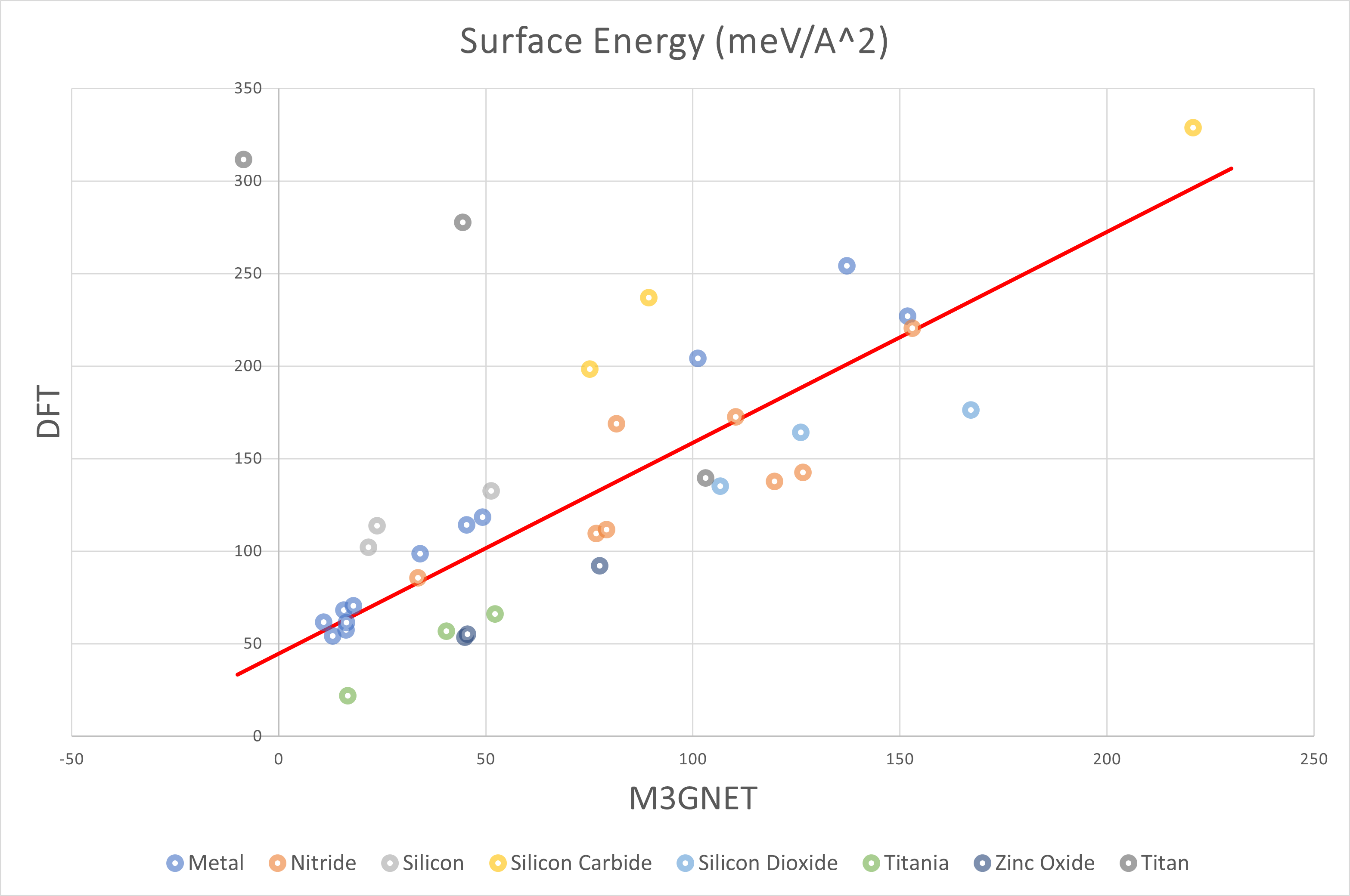
The above figure plots the surface energy with the DFT results on the vertical axis and the M3GNet results on the horizontal axis. The overall trend was a positive correlation, and M3GNet tended to estimate surface energies smaller than DFT calculations.
The table below summarized the structures for which the energy was an outlier or for which the DFT calculations did not converge.
| Material | Slab | EM3GNet (meV/Å2) | EDFT (meV/Å2) |
|---|---|---|---|
| Ti | (001) | 44.5 | 277.5 |
| Ti | (100) | 103.2 | 139.5 |
| Ti | (110) | -8.5 | 311.6 |
| TiN | (111) | Not converged |
Slab models containing unoxidized Ti were prone to outliers, and DFT calculations did not converge for TiN.
The following table shows the results using the least squares method for all structures except those above.
EDFT = a EM3GNet + b (meV/Å2)
s2: unbiased variance
| Group | a | b | s |
|---|---|---|---|
| All | 1.14 | 44.70 | 36.02 |
| Metal | 1.40 | 44.71 | 13.01 |
| Nitride | 0.94 | 52.20 | 25.33 |
| Oxide | 1.10 | 8.05 | 9.43 |
Interface Energy for Interface Model#
Analysis Procedure#
M3GNet was applied to interface models of several materials. The surface structures with vacuum layers on the top and bottom removed were optimized using M3GNet with anisotropically deforming the cell, then the energies were calculated in M3GNet and Quantum Espresso, respectively. The interface energies were calculated by subtracting the bulk energies by the number of atoms from the energy of the interface structure.
Structure Creation#
Advance/NanoLabo Pro feature made it easy to create interface models. The vacuum layer of the interface model was removed and adjusted to be continuous as a bulk. Interface models were created for metal/metal, metal/semiconductor, metal/insulator, semiconductor/semiconductor, semiconductor/insulator, and insulator/insulator, respectively, using the materials shown in the bulk models.
The following table shows the interface structures created.
Metal
| Material 1 | Material 2 |
|---|---|
| Au(001) | Al(001) |
| Au(001) | Pt(111) |
| Ti(001) | Al(111) |
Nitride(* different interface structures)
| Material 1 | Material 2 |
|---|---|
| AlN(001) | GaN(001)* |
| AlN(001) | GaN(001)* |
| AlN(001) | GaN(001)* |
| AlN(001) | SiC(111)* |
| AlN(001) | SiC(111)* |
| AlN(100) | GaN(100)* |
| AlN(100) | GaN(100)* |
| TiN(001) | W(001) |
Silicon
| material 1 | material 2 |
|---|---|
| Si(001) | SiO2(001) |
| Si(100) | Al(100) |
| Si(100) | Au(100) |
| Si(110) | Al2O3(100) |
| Si(111) | Al(111) |
| Si(111) | Au(111) |
| Si(111) | SiO2(111) |
Silicon Carbide
| material 1 | material 2 |
|---|---|
| Si(111) | SiC(111) |
Silicon Dioxide
| Material 1 | Material 2 |
|---|---|
| SiO2(100) | Al(100) |
| SiO2(100) | Au(100) |
Titania
| Material 1 | Material 2 |
|---|---|
| TiO2(001) | Au(100) |
| TiO2(001) | Ti(100) |
| TiO2(100) | Al(110) |
| TiO2(101) | Al(111) |
| TiO2(110) | Al2O3(100) |
Zinc Oxide
| Material 1 | Material 2 |
|---|---|
| ZnO(001) | Al(111) |
| ZnO(001) | Al2O3(100) |
| ZnO(110) | Al(110) |
| ZnO(110) | Pt(110) |
Analysis Result#
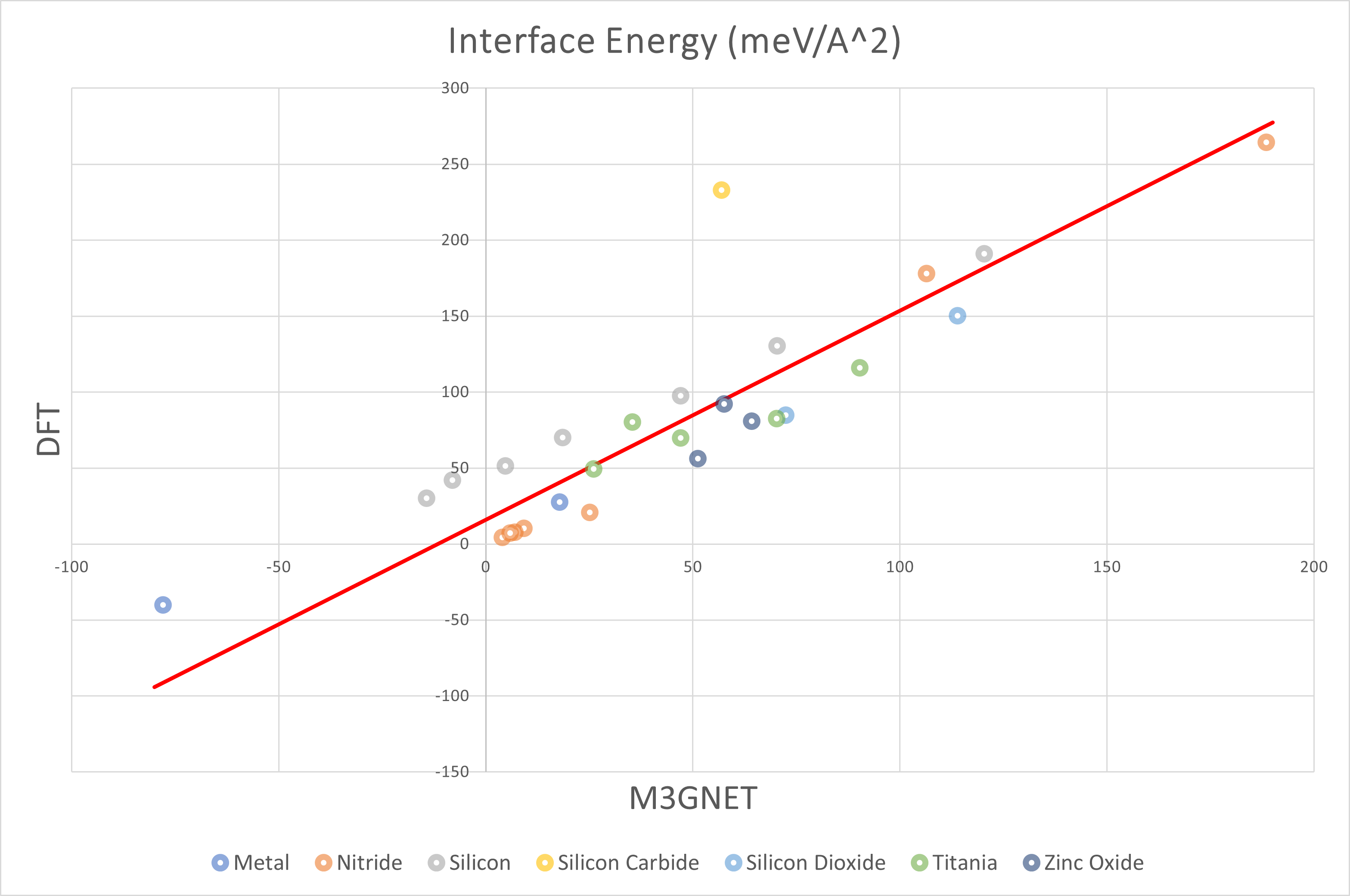
The above figure plots the interface energy with the DFT results on the vertical axis and the M3GNet results on the horizontal axis. The overall trend was a positive correlation, and M3GNet tended to estimate interface energies smaller than DFT calculations.
The table below summarized the structures for which the energy was an outlier or for which the DFT calculations did not converge.
| Material 1 | Material 2 | EM3GNet (meV/Å2) | EDFT (meV/Å2) |
|---|---|---|---|
| Si(111) | SiC(111) | 56.9 | 232.8 |
| Ti(001) | Al(111) | -60.5 | 2185.0 |
| ZnO(110) | Pt(110) | Not converged |
As in the surface models, interface models containing unoxidized Ti were prone to outliers. In this case, the calculation did not converge for the ZnO(110)-Pt(110) model. Besides, the offset of about 50meV/Å2 was observed between DFT and M3GNet for the silicon system. Particularly, the discrepancy between DFT and M3GNet was noticeable in the silicon carbide system.
The following table shows the results using the least squares method for all structures except those above.
EDFT = a EM3GNet + b (meV/Å2)
s2: unbiased variance
| Group | a | b | s |
|---|---|---|---|
| All | 1.38 | 15.85 | 25.47 |
| Silicon | 1.18 | 47.30 | 2.93 |
| Nitride | 1.55 | -4.97 | 12.47 |
| Oxide | 1.02 | 22.40 | 12.40 |
Summary#
This time, surface energies and interface energies were evaluated using M3GNet. In both cases, positive correlation was observed between M3GNet and DFT although M3GNet tended to estimate the energy smaller than DFT. Linear regression for all structures except those for which the energy was an outlier or for which the DFT calculations did not converge yielded 36meV/Å2 for surface energy, 25meV/Å2 for interface energy in terms of standard deviations of the error against DFT. Surface model yields larger errors because M3GNet is a machine learning potential trained on bulk structures.
These results indicate that M3GNet can be used for screening of material candidates.